Double Layer PCB


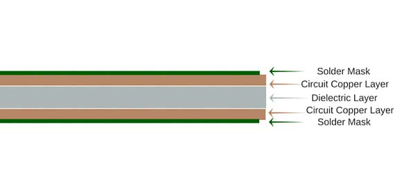
Double Layered printed circuit board technology is conceivably the most popular type of PCB in the industry. Double Sided PCB (also known as Double-Sided Plated Thru or DSPT) circuits are the gateway to advanced technology applications. They allow for a closer (and perhaps more) routing traces by alternating between top and bottom layers using vias.
Benefits of Double Sided PCBs
⦁ More Flexible to Design
⦁ Increased Circuit Compactness
⦁ Relatively Cost-Effective
⦁ Transitional Level of Circuit Density
⦁ Compact Board Size (which can reduce costs)
SR SPECIFICATIONS
1. Minimum conductor width 6 mils( 0.15 mm)
2. Minimum conductor Spacing/Air gap 6 mils( 0.15 mm)
3. Minimum Plated hole size 16 mils( 0.4mm)
4. Maximum Plated hole size 240 mils( 6mm)
5. Maximum board size 300 mm x 350 mm
6. Maximum number of layers 2
7. Minimum copper thickness 1 Oz (35 microns)
8. Maximum copper thickness 3 Oz (105 microns)
9. Dedicated Electrical Testing (BBT) Available
10. PCB Cutting options Routing , V groove , Punching
Product Finish
SR SPECIFICATIONS STANDARD
1. Single Sided HAL, Lacquer
2. Double Sided HAL, TIN , Electroplated Gold & Nickel
3. Solder Mask Finish PISM, Liquid Solder Mask
4. Solder Mask color Green, White, Black, Blue ,Red
5. Legend/Ident color White, Black, yellow, Green
6. Special Requirement Carbon Printing on Push Button , Selective Gold & Nickel plating on Connecting Tabs
Product Raw Material
SR SPECIFICATIONS STANDARD
1. Single Side FR1,FR4, CEM1,CEM3, PP, Metal Clad
2. Double Side FR4
3. Board Thickness (in mm) 0.4 , 0.8 ,1.0 , 1.2, 1.6 ,2.4 , 3.2
