Multi Layer PCB
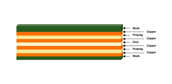
Multilayer PCB is made up of more than two layers using conductive copper foils and prepreg material, pressed and bonded together. Multilayer is most complex printed circuit board by design and by manufacturing. Nowadays, up to 40 layers of multilayer PCB is possible to manufacture using advanced machinery. ProtoPCBhas capabilities to make multilayer PCB up to 6 layers.
Multilayer PCBs are complex to manufacturer but high speed by functionally. Multilayer PCB are mainly used professional electronic equipment like computer, mobile, medical devices, aerospace and defense application devices.
Benefits of Multilayer PCBs (compared to single or double-sided PCBs)
⦁ Higher Assemblage Density
⦁ Reduced Size (considerable savings on space)
⦁ Enhanced Flexibility
⦁ Easier Incorporation Controlled Impedance Features
⦁ EMI Protecting through Careful Placement of Power and Ground Layers
⦁ Reduced need for Interconnection (Wiring Joints reducing the overall weight)


SR SPECIFICATIONS
1. Minimum conductor width 6 mils(0.15 mm)
2. Minimum conductor Spacing/Air gap 6 mils(0.15 mm)
3. Minimum Plated hole size 16 mils(0.4mm)
4. Maximum Plated hole size 240 mils(6mm)
5. Maximum board size 380 mm x 280 mm
6. Maximum number of layers 6
7. Minimum copper thickness 1 Oz(35 microns)
8. Maximum copper thickness 3 Oz(105 microns)
9. Dedicated Electrical Testing BBT, Flying Probe
10. PCB Cutting options Routing, V-Groove, Punching
Product Finish
SR SPECIFICATIONS
1. Single Sided HAL, Lacquer
2. Double Sided HAL, Electroplated Gold & Nickel
3. Solder Mask Finish PISM, Liquid Solder Mask
4. Solder Mask color Green, White, Black, Blue ,Red
5. Legend/Ident color White, Black
6. Special Requirement Carbon Printing on Push Button , Selective Gold & Nickel plating on Connecting Tabs
Product Raw Material
SR SPECIFICATIONS
1. Single Side FR1,FR4, CEM1,CEM3, PP, Metal Clad
2. Double Side FR4
2. Board Thickness (in mm) 0.4 , 0.8 ,1.0 , 1.2, 1.6 ,2.4 , 3.2
