Single Layer PCB
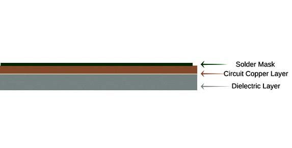
Single Layer PCBs have been around since the late 1950s and still dominate the world market in sheer piece volume. Single Sided PCBs contain only one layer of conductive material and are best suited for low-density designs. Single Layer PCBs are easy to design and quick to manufacture. They serve as the most lucrative platform in the industry.
Benefits of Single Layer PCBs:
⦁ Perfect for simple low-density designs
⦁ Lesser cost, especially for high volume orders
⦁ Lesser chance of manufacturing issues
⦁ Popular, common, and easily comprehensible by most PCB manufacturers
SR SPECIFICATIONS
1. Minimum conductor width 6 mils( 0.15 mm)
2. Minimum conductor Spacing/Air gap 6 mils( 0.15 mm)
3. Minimum Plated hole size 16 mils( 0.4mm)
4. Maximum Plated hole size 240 mils( 6mm)
5. Maximum board size 250 mm x 350 mm
6. Maximum number of layers 10
7. Minimum copper thickness 1 Oz (35 microns)
8. Maximum copper thickness 3 Oz (105 microns)
9. Dedicated Electrical Testing (BBT) Available
10. PCB Cutting options Routing , V groove
Product Finish
SR SPECIFICATIONS STANDARD
1. Single Sided HAL, Lacquer
2. Double Sided HAL, Electroplated Gold & Nickel
3. Solder Mask Finish PISM
4. Solder Mask color Green, White, Black, Blue ,Red
5. Legend/Ident color White, Black, yellow, Green
Product Raw Material
SR SPECIFICATIONS STANDARD
1. PCB Base material FR1,FR4, CEM1,CEM3,Metal Clad
2. Board Thickness (in mm) 0.8 to 3.2 mm


